Journal of Applied Science and Engineering

Published by Tamkang University Press

1.30

Impact Factor

2.10

CiteScore

I-Nan Lin  1,2, Yi-Ping Chou3 and Tong T. Chen3

1Department of Physics Tamkang University Tamsui, Taiwan 251, R.O.C.
2Material Science Center National Tsing Hua University Hsinchu, Taiwan 300, R.O.C.
3Department of Physics National Tsing Hua University Hsinchu, Taiwan 300, R.O.C.


Received: May 6, 2003
Accepted: June 10, 2003
Publication Date: September 1, 2003

Download Citation: ||https://doi.org/10.6180/jase.2003.6.3.02  


ABSTRACT


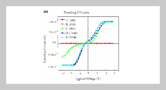
Effect of boron and nitrogen co-doping on the electron field emission properties of the diamond films was examined using current image tunneling spectroscopy in atomic force microscopy (CITS, AFM). Tunneling current-voltage (It-V) characteristics measured by AFM indicate that incorporation of boron and nitrogen species induced the presence of impurity state. Such a characteristic is closely related to the local electron field emission behavior of the diamond films. The samples co-doped with 4 sccm boron and 3 sccm nitrogen possess smallest energy gap (Eg = 1.62 eV) and largest emission ratio, as compared with that of other diamond films. These diamond films can be turned on at smallest electric field (Eo = 6.4 V/µm), exhibiting largest field emission capacity (Je = 1,500 µA/cm2 ).


Keywords: Co-doped Diamond Films, Electron Field Emission Properties, Current Image Tunneling Spectroscopy


REFERENCES


  1. [1] Spindt, C. A.; Brodie, I.; Humphrey, L.; Westerberg, E. R. J. Appl. Phys. 1976, 47, 5248.
  2. [2] Van Gorkom, G. G. P.; Hoeberechts, A. M. E. J. Vac. Sci. Technol. B 1986, 4, 108.
  3. [3] Himpsel, F. J.; Knapp, J. A.; Van Vechten, J. A. Phys. Rev. 1979, 20, 624.
  4. [4] Zhu, W.; Kochanski, G. P.; White, A. E. Appl. Phys. Lett. 1995, 68, 1157.
  5. [5] Ku, T. K.; Chen, S. H.; Cheng, H. C. IEEE Elec. Device Lett. 1996, 17, 208.
  6. [6] Glesener, J. W.; Morrish, A. A. Appl. Phys. Lett. 1996, 69, 785.
  7. [7] Okano, K.; Koizumi, S.; Silva, SRP.; Amaratunga, G. Nature 1996, 381, 140.
  8. [8] Okano, K.; Gleason, K. K. Electronics Lett. 1995, 31, 74.
  9. [9] Geis, M. W.; Twichell, J. C.; Lyszczarz, T. M. Appl. Phys. Lett. 1996, 68, 2294.
  10. [10] Hong, T. M.; Chen, S. H.; Chiou, Y. S.; Chen, C. F. Appl. Phys. Lett., 1995, 67, 2149.
  11. [11] W. Muller Cebert, Worcer, E.; Fuchs, F.; Wiland, C.; Koide, P. Appl. Phys. Lett. 1996, 68, 759.
  12. [12] Won, J. H.; Hatta, A.; Yagyu, H.; Jiang, N.; More, Y.; Ito, T.; Sasaki, T.; Hiraki, A. Appl. Phys. Lett. 1996, 68, 2822.
  13. [13] Chen, Y. H.; Hu, C. T.; Lin, I. N.; J. Appl. Phys. 1998, 84, 3890.
  14. [14] Shih, C. F.; Liu, K. S.; Lin, I. N. Diam. Rel. Mater. 2000, 9, 1591.
  15. [15] Vander Z. Solid State Physical Electronics; Prentice-Hall: Englewood Cliffs, NJ, U.S.A., 1968, 144.


Latest Articles