T. K. Shing This email address is being protected from spambots. You need JavaScript enabled to view it.1, H. H. Pan1, I.-C Chen1 and C. I. Kuo1 1Material Research Laboratory Industrial Technology Research Institute Jhudong, Taiwan 310, R.O.C.
Received:
December 29, 2003
Accepted:
January 16, 2004
Publication Date:
September 1, 2004
Download Citation:
||https://doi.org/10.6180/jase.2004.7.3.02
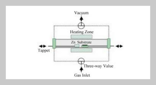
ZnO nanowires provide enormous advantages such as high aspect ratio, good field electron emission property and excellent molecular absorption and desorption characteristics in catalyst applications. Fabrication technologies with nanometer resolution will enable us to realize complex solid state devices with novel mechanical, electronic or optical functions. In this paper, two most popular substrates, silicon and LiNbO3, are chosen for the study on such integration issues. The influences from substrate, process procedures and etching solutions on the growth and patterning of ZnO nanowires are discussed. The results are quite promising.ABSTRACT
Keywords:
ZnO, Nanowire, Integration, Patterning.
REFERENCES
